- 您现在的位置:买卖IC网 > Sheet目录969 > CDB4353 (Cirrus Logic Inc)BOARD EVAL FOR CS4353 DAC
�� �
�
�CDB4353�
�5.� POWER� SUPPLY� CIRCUITRY�
�Power� is� supplied� to� the� evaluation� board� by� two� binding� posts,� GND� and� +3.3� V� (see� Figure� 33� ).� The� allowable�
�input� voltage� range� for� the� binding� posts� is� 3.13� V� to� 3.47� V.� The� VL� supply� can� be� connected� to� the� +3.3� V� binding�
�post� by� shunting� J1� or� provided� externally� by� removing� the� shunt� on� J1� and� connecting� another� voltage� to� pin� 2� of�
�J1� (labeled� VL).� VCP� and� VA� are� normally� supplied� by� the� 3.3� V� binding� post� but� can� be� set� to� separate� voltages�
�by� removing� the� shunts� on� J8� and� J10,� removing� R9� and� R14,� and� then� applying� external� voltages� to� pin� 1� of� J8�
�and� J10.�
�Power� consumption� of� the� CS4353� can� be� measured� through� the� voltage� drop� at� J8,� J9,� and� J10� when� the� shunts�
�are� removed.�
�WARNING:� Refer� to� the� CS4353� datasheet� for� maximum� allowable� voltages� levels.� Operation� outside� of� this� range�
�can� cause� permanent� damage� to� the� device.�
�6.� GROUNDING� AND� POWER� SUPPLY� DECOUPLING�
�As� with� any� high-performance� converter,� the� CS4353� requires� careful� attention� to� power� supply� and� grounding� ar-�
�rangements� to� optimize� performance.� Figure� 32� details� the� connections� to� the� CS4353� and� Figures� 34� ,� 35� ,� and� 36�
�show� the� component� placement� and� top� and� bottom� layout.� The� decoupling� capacitors� are� located� as� close� to� the�
�CS4353� as� possible.�
�7.� HARDWARE� CONTROL�
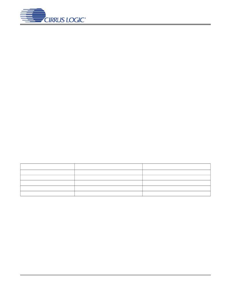
�The� CDB4353� is� controlled� through� settings� on� switch� S1.� This� allows� for� configuration� of� the� board� without� a� PC.�
�Switch� S1� can� toggle� settings� for� CS8416� MCLK� speed,� CS8416� and� CS4353� PCM� data� format,� clock� and� data�
�source� for� the� board,� and� the� Hardware� Mode� configuration� of� the� CS4353.� Table� 1� below� shows� S1� settings� for�
�S/PDIF� input� and� PCM� input� header� quick� setup� modes.� See� Table� 4� for� details� on� each� switch� S1� setting.�
�S1� POSITION�
�1�
�2�
�3�
�4�
�5�
�S/PDIF� INPUT� -� OPT1� or� J16�
�Up�
�Down�
�Down�
�Up�
�Down�
�PCM� INPUT� -� J3�
�Down�
�Down�
�Down�
�Up�
�Down�
�Table� 1.� Switch� S1� Quick� Setup�
�8.� CS8416� AND� CS4353� RESET�
�Pressing� switch� S2� resets� the� CS8416.� Jumper� J5� sets� whether� the� CS4353� is� reset� by� switch� S2� (External)� or� by�
�the� CS4353’s� internal� power-on� reset� function� (POR).�
�9.� ANALOG� OUTPUT� FILTERING�
�The� analog� output� on� the� CDB4353� has� been� designed� according� to� the� CS4353� datasheet.� This� output� circuit� con-�
�sists� of� a� single-pole� R� and� C� filter.� J11� selects� the� output� ground� reference� for� the� CS4353.� The� output� reference�
�can� be� set� to� the� evaluation� board’s� ground� (shunted)� or� J14� and� J15’s� ground� connection� (not� shunted).� See�
��DS803DB2�
�5�
�发布紧急采购,3分钟左右您将得到回复。
相关PDF资料
CDB4365
EVALUATION BOARD FOR CS4365
CDB4385
BOARD EVAL FOR CS4385 DAC
CDB43L22
BOARD EVAL FOR CS43L22
CDB5340
BOARD EVAL FOR CS5340 STEREO ADC
CDB5343
BOARD EVAL FOR CS5343 STEREO ADC
CDB5451A
EVAL BOARD CS5451A 6CH ADC
CDB5524
EVAL BOARD FOR CS5524 ADC
CDB5581
BOARD EVAL FOR CS5581 ADC
相关代理商/技术参数
CDB4354
功能描述:音频 IC 开发工具 Eval Board 5V DAC w/ 2Vrms line driver
RoHS:否 制造商:Texas Instruments 产品:Evaluation Kits 类型:Audio Amplifiers 工具用于评估:TAS5614L 工作电源电压:12 V to 38 V
CDB4360
功能描述:音频 IC 开发工具 Eval Bd 102dB 192kHz 6-Ch DAC
RoHS:否 制造商:Texas Instruments 产品:Evaluation Kits 类型:Audio Amplifiers 工具用于评估:TAS5614L 工作电源电压:12 V to 38 V
CDB4361
功能描述:音频 IC 开发工具 Eval Bd 105dB 192kHz 6-Ch DAC
RoHS:否 制造商:Texas Instruments 产品:Evaluation Kits 类型:Audio Amplifiers 工具用于评估:TAS5614L 工作电源电压:12 V to 38 V
CDB4362
制造商:Cirrus Logic 功能描述:Tools Development kit Kit Con
CDB4362A
功能描述:音频 IC 开发工具 Eval Bd 1142dB 24Bit 192kHz DAC
RoHS:否 制造商:Texas Instruments 产品:Evaluation Kits 类型:Audio Amplifiers 工具用于评估:TAS5614L 工作电源电压:12 V to 38 V
CDB4364
功能描述:音频 IC 开发工具 Eval Bd 6-Ch DAC w/DSD
RoHS:否 制造商:Texas Instruments 产品:Evaluation Kits 类型:Audio Amplifiers 工具用于评估:TAS5614L 工作电源电压:12 V to 38 V
CDB4365
功能描述:音频 IC 开发工具 Eval Bd 6-Ch DAC w/DSD
RoHS:否 制造商:Texas Instruments 产品:Evaluation Kits 类型:Audio Amplifiers 工具用于评估:TAS5614L 工作电源电压:12 V to 38 V
CDB4382
制造商:Cirrus Logic 功能描述:Tools Development kit Kit Con